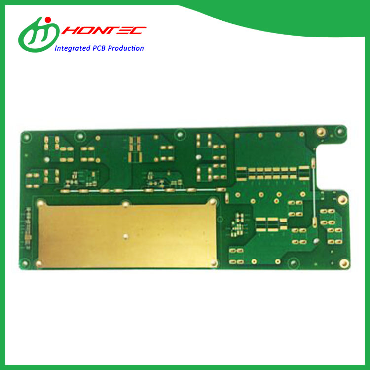

Components of inlaid copper coin PCB
2023-11-15
An inlaid copper coin PCB refers to a printed circuit board (PCB) that incorporates a copper coin or a copper layer in a specific design or configuration. This might involve embedding a copper coin within the PCB structure for functional or aesthetic purposes. Let's break down the components of this term:
1. Inlaid Copper:
- "Inlaid" refers to the process of embedding one material into another. In this context, copper is likely embedded within the PCB structure.
2. Copper Coin:
- A copper coin, in this case, could be a literal coin made of copper, or it could refer to a copper layer or shape designed to resemble a coin.
3. PCB (Printed Circuit Board):
- A PCB is a board made of insulating material with conductive pathways (traces) etched or printed onto the surface to connect various electronic components. PCBs are used in almost all electronic devices to provide a platform for the assembly and connection of electronic components.
The combination of these elements suggests a unique or specialized PCB design where a copper coin or layer is incorporated into the board. Here are some potential scenarios for the use of an inlaid copper coin in a PCB:
1. Aesthetic Design:
- The copper coin may serve a decorative or branding purpose, providing a distinctive appearance for the PCB. This could be relevant in consumer electronics or other products where the visual design is important.
2. Thermal Dissipation:
- Copper is an excellent conductor of heat. In some cases, an inlaid copper layer might be strategically placed to enhance the PCB's thermal dissipation capabilities, helping to dissipate heat generated by electronic components.
3. Electromagnetic Interference (EMI) Shielding:
- Copper is also effective at blocking electromagnetic interference. Incorporating a copper coin for shielding purposes can help reduce the impact of electromagnetic interference on the components on the PCB.
4. Customization and Branding:
- Some companies might use inlaid copper coins with their logos or other branding elements to create a unique identifier for their products.
5. Functional Integration:
- Depending on the design, the copper coin might serve a functional purpose, such as providing a ground plane, acting as an antenna, or serving as a part of a larger circuit.
The specific application and purpose of an inlaid copper coin in a PCB would depend on the requirements of the electronic device, the desired functionality, and any specific design considerations. Custom PCB manufacturers with specialized capabilities may be involved in producing such boards based on the unique requirements of the design.